Reflective surfaces
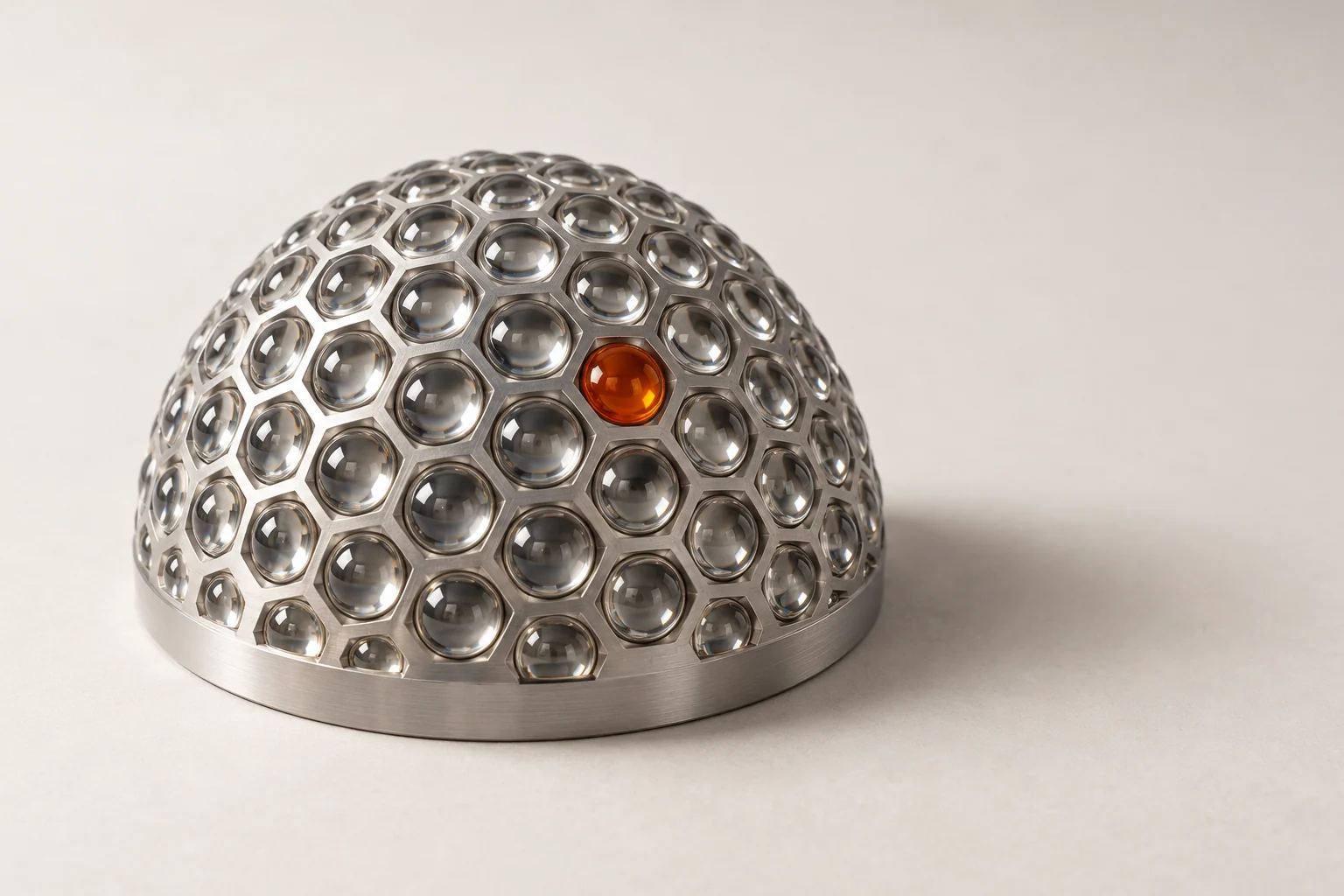
Dome and coaxial illumination remove specular glare. Deflectometry — a known pattern reflected in the surface — turns small dents and waviness into visible distortion.
Edge Hardware
Mirror-finish metal, clear glass, glowing steel, product moving too fast to freeze. We design the optics, illumination and housing that make the defect visible, then build the sensor — from first prototype to small production runs.
The problem
Standard smart cameras assume a matte part, steady room light and a clear line of sight. Plenty of real applications break all three. On a polished housing the camera sees a reflection of the ceiling, not the dent. In a clear vial, a crack is a faint change in how light bends. A billet leaving a furnace glows brighter than any light you can point at it. Inside a machine there may be 60 mm between the product and the nearest guard.
No model can find a defect that is not in the pixels. When a camera trial produces images where an experienced inspector cannot see the defect either, the answer is not more training data. It is optics: the right light, from the right angle, at the right wavelength, through a housing that survives the environment.
How it works
Dome and coaxial illumination remove specular glare. Deflectometry — a known pattern reflected in the surface — turns small dents and waviness into visible distortion.
Dark-field lighting, backlighting and polarization reveal cracks, bubbles, particles and stress in glass, film and clear plastics.
Short-wavelength light with narrow-band filters outshines the glow of hot metal. Cooled or air-purged housings keep scale and heat off the optics.
IP69K 316L stainless housings with sealed windows and no ledges where product can collect, for food and pharmaceutical hygiene zones.
Remote sensor heads and folded optical paths with mirrors or prisms fit where a camera body will not, with the electronics mounted somewhere serviceable.
Microsecond strobes freeze motion; line-scan sensors synchronized to an encoder image continuous webs and products moving too fast for area cameras.
The optics lab
Our optics lab in Jackson is run by Samuel Achterberg, our Principal Optical Engineer. It is where every Feasibility Sprint starts: your parts are imaged under bright-field, dark-field, dome, coaxial, backlit and structured illumination, at several wavelengths and angles, and the contrast of each defect is measured rather than judged by eye.
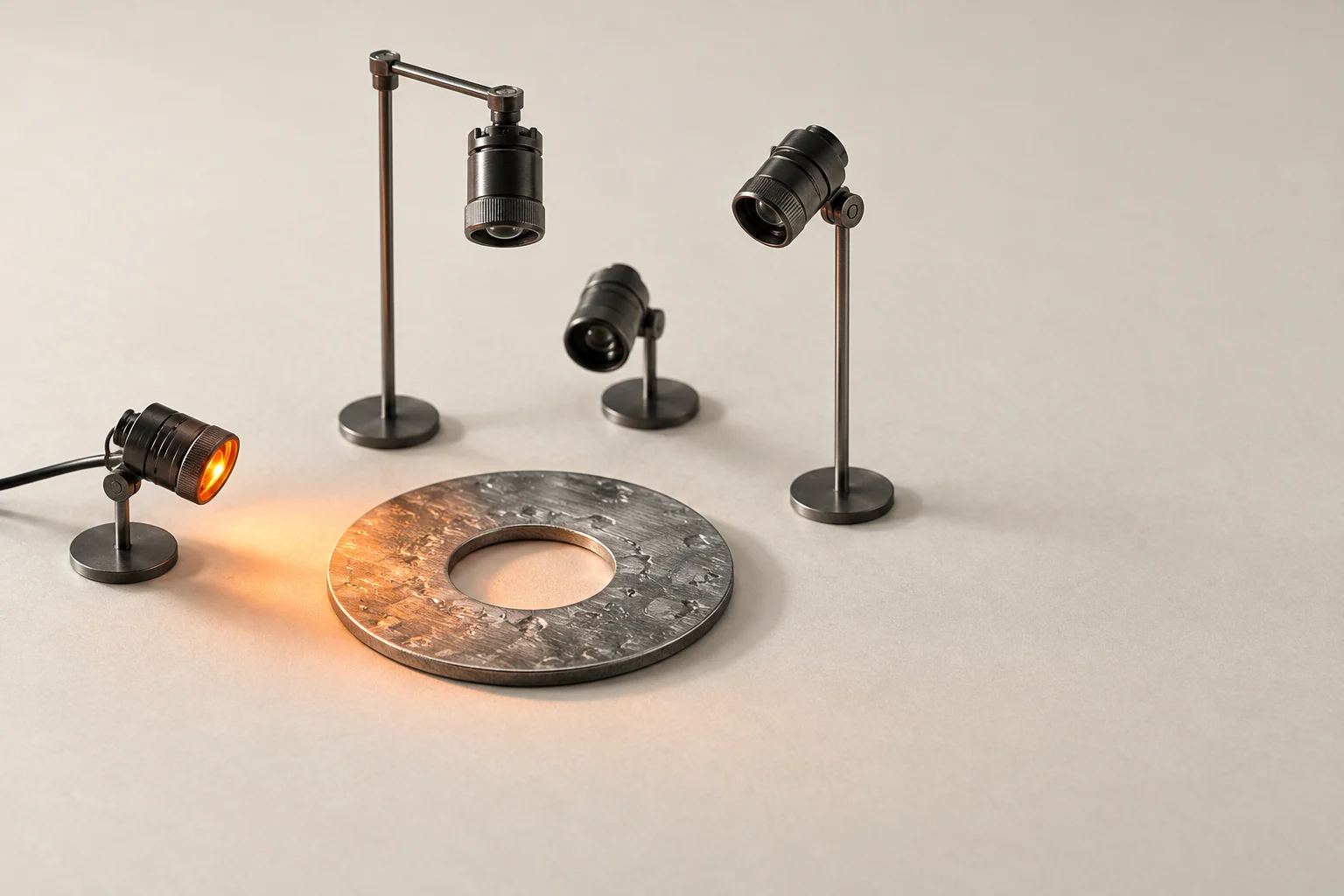
When no standard combination works, the lab is also where custom sensors begin — machined adapters, printed fixtures and optical breadboards that prove a design on real parts before any housing is drawn. Prototypes then run on a conveyor rig at representative speed, so the strobe timing and exposure are tested in motion, not on a bench.
Process
Your good and defective parts are imaged under many geometries in our lab. You get sample images, measured contrast per defect and a written go/no-go.
Lens, illumination, filters, geometry and housing are specified, with the trade-offs written down — field of view against resolution, speed against light budget.
A working sensor is built, tested on the conveyor rig, then installed on your line or in your machine to confirm image quality in real conditions.
Pilot units, then small production runs, each tested against the image-quality criteria agreed at the prototype stage.
Deliverables
Building blocks
Honest fit
See it in context
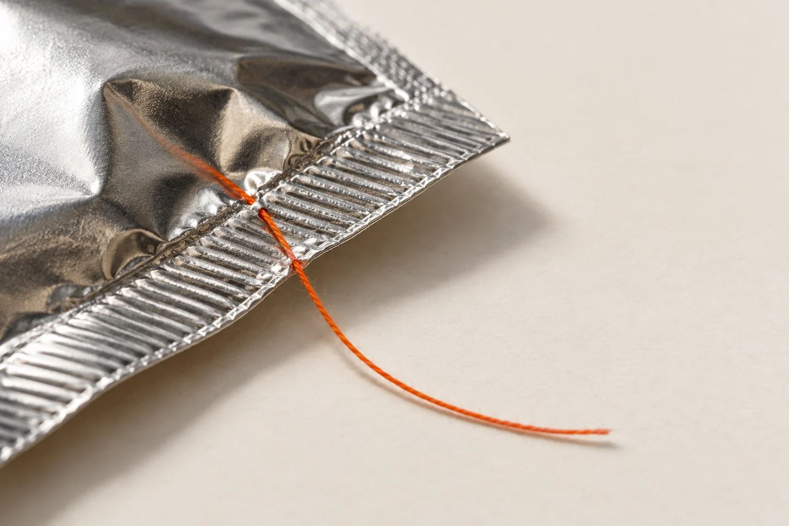
Low-angle red light turns a leaking seal channel into a visible shadow in a modeled food-line scenario.
Read more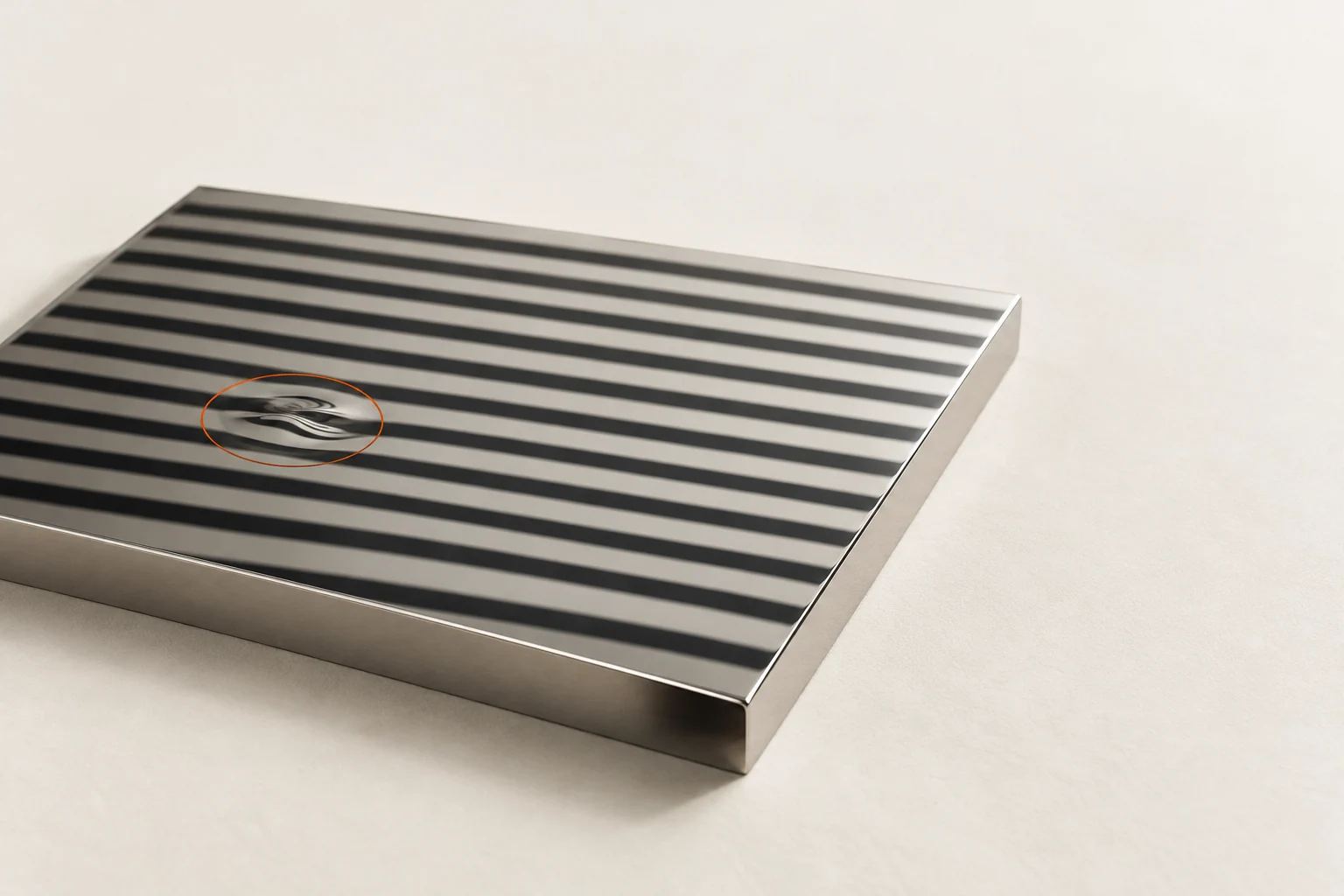
Polished, oily and hot surfaces where reflections and glow hide the defect from ordinary cameras.
Read more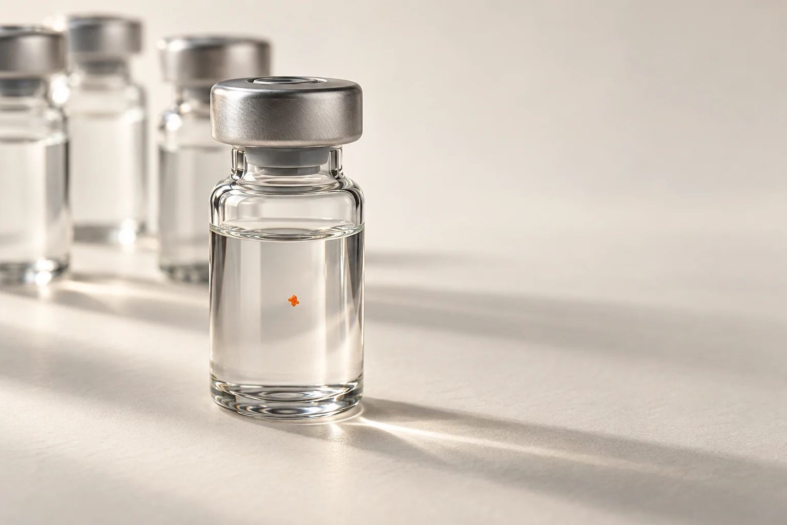
Clear vials, syringes and blister packs where defects show up only under the right light.
Read moreFAQ
Often just a better light. We always try standard lenses and illumination first in the Feasibility Sprint; a custom sensor is only proposed when the measured contrast says standard parts cannot do the job.
Lensnode sensors run from −20 to 55 °C as standard. Beyond that we design cooled or air-purged housings, or keep the electronics farther away and bring the image to them through optics.
Yes. We design, prototype and build pilot units and small production runs for equipment makers, with drawings and test procedures that support larger builds. Firmware and boards come from our embedded engineering team.
They help us prepare, but they cannot replace real parts. The whole point of the lab is to see how the defect responds to different light, and that needs the physical sample.
The Feasibility Sprint answers in 3 weeks whether the defect can be made visible and with what. The timeline for prototype and pilot units depends on the design and is set out in the written proposal that follows.
Ship us samples. In three weeks our optics lab tells you whether the defect can be made visible, and with which light, lens and housing.